Dren Qerimi
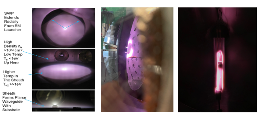
Extreme ultraviolet (EUV) lithography tools are the leading technologies responsible for the next generation of chip manufac- turing. EUV has shown to accurately and precisely pattern wafers but still lags in the wafer production rate compared to previous high-volume manufacturing. Source availability is a key issue to be addressed in order to achieve a higher speed.1 In an EUV source, a plasma is generated when a CO2 pulsed laser hits molten droplets of tin, and it ionizes tin in the +8 to +12 range, which then emit 13.5 nm photons. A multilayer mirror (MLM) collector reflects the light toward a series of optic mirrors until EUV lights reaches the wafer.2 During de-excitation of the Sn plasma, droplets and atoms of Sn deposit on the inner surfaces of the source, including the walls and the collector mirror. Sn film deposits absorb 13.5nm photons, reducing the reflectivity that leads to severe drop in source power at the wafer. Conventional Sn cleaning is a multiday process, thus causing major downtime for the tool. An in situ tin etch method increases lifetimes of the EUV source including collector and plasma facing components. One advantage of using hydrogen gas inside an EUV source is that hydrogen radicals are produced and chemically etch Sn away to form tin hydride.3 Having shown previously the ability of tin etching in hydrogen plasmas4 and recov- ery of near total reflectivity,5 this study shows Sn removal from any surface in an EUV source as a function of surface temperature. Also, previous work has shown that the highest etch rates occur when plasma is in the reactive ion etch regime. A linear surface wave plasma (SWP) is used replicating actual source conditions (pressure, gas flow rate, and geometry) in the Illinois NXE:3100 system. SWP has high hydrogen radical and ion densities, while electron and ion energies are low in order to avoid damage to the MLM. Very high etch rates have been observed, up to 200nm/min with ion and radical densities on the order of 10^12 to10^13 cm3 and 10^14 cm3, respectively. A custom launcher and an antenna structure were built to interface with the present source geometry. At CPMI, we have tested semi-circular SWP antennas with etch rates as high at 270nm/min.
1. Button Source Source 2. Two semi-circular SWP sources 3. Linear SWP