 SHADE has two 4-inch PVD sputtering guns, a load-lock and a rotating sample stage. It is also outfitted with detailed diagnostics to enable time-resolved measurements of HIPIMS discharges. It is powered by a Starfire Industries IMPULSE that is capable of cathode-voltage reversal. It has been used to make multi-layer mirrors, and do reactive sputtering experiments.
The company COMET makes advanced RF power supplies capable of fast-turn on and matching. We will be using one of their supplies in an ICP configuration and measuring the time-resolved plasma conditions to correlate the to the settings of the power supply.
 This is a PVD sputtering tool manufactured by the Material Research Corporation (MRC). It uses a 14 inch diameter target and a rotating magnet pack. We have outfitted it with a variety of HIPIMS power supplies, used a variety of magnet packs, diagnostics and internal ionization coils.
 ECAP is a microwave-powered atmospheric-pressure plasma torch. It has three zones where reactants can be introduced to the plasma. In this way it can make a variety of coatings, which would normally require a vacuum system to produce.
 When a femtosecond laser pulse hits a surface, the power is incredible. It is so intense that it instantly turns the surface into a plasma even before the laser pulse ends. This means there is a chance that the laser light is converted to surface plasmons, and they will deposit their energy as a constructively interfered wave. This leads to ripples on the surface with dimensions near the wavelength of the initial laser. This texturing can be used for photonic properties, or to alter the wetting of the surface. We learned that such ripples can prevent wetting of metal surfaces by lithium.
 XCEED is an XTS-13-35 EUV source made by Xtreme Technologies. The same model source was used to make the very first chips that used EUV lithography in INTEL’s MET tool. It uses a discharge-produced plasma from a Z-pinch and puts 5 J of energy into the plasma in 5ns. This device will be re-purposed to study warm-dense matter in a project funded by Los Alamos National Laboratory.
The Mock Entry Module for East (MEME), a 1.2m x 1.2m x 1.2m vacuum system, is a replica of the energy module for the EAST tokamak in China and is used for molten lithium experiments and diagnostic development.
The experiment will involve the design and implementation of a vacuum oven to produce clean samples of SnLi alloys at multiple mass ratios. The samples’ material properties will then be examined, which include surface wetting and vapor pressure.
I am currently researching how tin ions are stopped as they travel through hydrogen plasma. Tin plasmas are generated during the production of extreme ultraviolet light (EUV) when molten microdroplets of tin are struck by a CO2 laser. The contamination of critical vessel components with tin is a serious concern for ASML, the project sponsor, and they are interested in learning more about how ions from the tin plasma are stopped by the background gases and plasmas in their vessel. I am currently using an ion beam installed on the chamber to measure how an ion beam attenuates as it travels through both hydrogen gas as well as hydrogen plasma generated by a helicon plasma source.
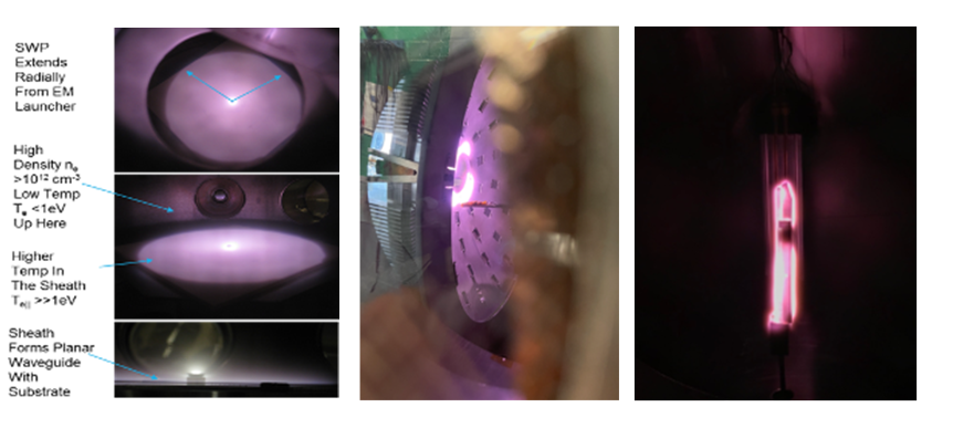
Extreme ultraviolet (EUV) lithography tools are the leading technologies responsible for the next generation of chip manufacturing. EUV has shown to accurately and precisely pattern wafers but still lags in the wafer production rate compared to previous high-volume manufacturing. Source availability is a key issue to be addressed in order to achieve a higher speed.1 In an EUV source, a plasma is generated when a CO2 pulsed laser hits molten droplets of tin, and it ionizes tin in the +8 to +12 range, which then emit 13.5 nm photons. A multilayer mirror (MLM) collector reflects the light toward a series of optic mirrors until EUV lights reaches the wafer.2 During de-excitation of the Sn plasma, droplets and atoms of Sn deposit on the inner surfaces of the source, including the walls and the collector mirror. Sn film deposits absorb 13.5nm photons, reducing the reflectivity that leads to severe drop in source power at the wafer. Conventional Sn cleaning is a multiday process, thus causing major downtime for the tool. An in situ tin etch method increases lifetimes of the EUV source including collector and plasma facing components. One advantage of using hydrogen gas inside an EUV source is that hydrogen radicals are produced and chemically etch Sn away to form tin hydride.3 Having shown previously the ability of tin etching in hydrogen plasmas4 and recovery of near total reflectivity,5 this study shows Sn removal from any surface in an EUV source as a function of surface temperature. Also, previous work has shown that the highest etch rates occur when plasma is in the reactive ion etch regime. A linear surface wave plasma (SWP) is used replicating actual source conditions (pressure, gas flow rate, and geometry) in the Illinois NXE:3100 system. SWP has high hydrogen radical and ion densities, while electron and ion energies are low in order to avoid damage to the MLM. Very high etch rates have been observed, up to 200nm/min with ion and radical densities on the order of 10^12 to10^13 cm3 and 10^14 cm3, respectively. A custom launcher and an antenna structure were built to interface with the present source geometry. At CPMI, we have tested semi-circular SWP antennas with etch rates as high at 270nm/min.