PACE – Plasma Assisted Cleaning by Electrostatics
February 27, 2009Objective Statement
The goal of PACE is to show how a helium plasma can reduce or eliminate organic contamination from materials used in extreme ultraviolet lithography.
Why PACE Has Taken on This Task
Reliability and speed in computing are two key aspects that continue to drive the economic and personal lives of individuals in today’s society. These two key aspects of computing are achieved through the continued development and refinement of the way in which integrated circuits (IC) are manufactured. In order to obtain more functionality out of a computer chip, more transistors are needed on that chip compared to previous generations. This proves to be a difficult hurdle to overcome, either the features (transistors) need to become smaller to fit more of them into the same amount of real-estate, or the chip needs to become physically larger and thus leads to larger devices. The trend has been to decrease the size of the transistors to increase the number of them per chip, however, this presents many complications for the design and fabrication engineers. In 1965, Gordon Moore made the observation that the number of transistors on a chip would double every two years [1]. To keep the trend now referred to as Moore’s law applicable, the shift to extreme ultraviolet lithography (EUVL) at 13.5 nm is seen as one solution in order to achieve this [2]. The idea of EUVL has led to a huge scientific undertaking by both private industry and Universities in order to produce the concepts and machines capable of making EUVL possible. There have been numerous challenges in both optical design, source design, photoresist sensitivity, and lithographic mask that have stood in the way as hurdles to EUVL’s implementation [2]. The subject of a lot of these hurdles has led to great advances in science and engineering, as well as aided numerous students to partake in research and development for both academic and industrial purposes. EUVL has the potential to be the next large step and revolutionize the way IC’s are manufactured. The ability to manufacture IC’s with a direct pattern technique instead of phase-shift masks or double patterning, as is the current path of IC manufacturing with current 193 immersion technology, will provide IC designers with more tools and abilities in the design of IC’s to further their applicability to the desire for increased computing power. One of the largest hurdles facing EUVL implementation is contamination in the EUVL system, particularly contamination of the photomask in the form of particulate defects and thin film contamination and carbon buildup and contamination of the collector optics. These key aspects need to be addressed and a high volume manufacturing solution determined before EUVL can be successfully implemented.
Contamination and Its Effect on EUVL
Integrated circuits are the combination of miniaturized electronic circuits and passive elements built into the surface of a semiconductor material such as silicon. There are several steps that are required to form an integrated circuit, these steps are: imaging, deposition, and etching [3]. To make a single device, several processing steps focused around the previously mentioned three are conducted. Supplementary steps such as cleaning and planarization[3] are also required to ensure the functionality of devices and to make the processing steps more precise.
EUV Lithography
As shown in Figure 1.1, there is no pellicle between the mask and the wafer due to the non-transparency of materials to 13.5 nm wavelength light. Also, the mask requires illumination from the side and at an angle due to the inability of a passthrough type design which is also due to the non-transparency of material to the 13.5 nm wavelength. Thus, whereas in an optical lithography system utilizing a transmissive mask, a pellicle can be used to reduce the number of defects that reach the mask, in an EUV system, this is less likely to be the case.
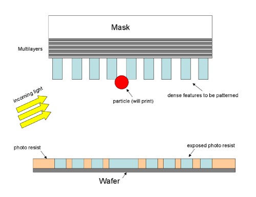
Figure 1.1: A diagram of a particle falling onto an EUV lithography mask. If the particle remains on the mask, then it will block light reflecting off of the mask and appear to be another feature not intended by the mask design which will cause errors and device failures.
The alternating light/dark layers beneath the dense features are the multilayers. The multi-layers are specifically designed to reflect EUV light. NOTE: the size of the wafer/resist are not to size but have been enlarged for clarity and the incoming light is not at as extreme an angle.
EUV Mask Fabrication
There is an additional issue for particle contamination when considering EUV lithography. In forming the alternating multilayers for the reflective properties of the EUV mask, particle control is important. As seen in Figure 1.2, if a particle falls onto the surface during multilayer deposition, the overall smoothness of the mask is affected. Thus, by effective particle and contamination control or an effective cleaning process, the mask smoothness before patterning can be maintained to provide a defect free mask during fabrication.
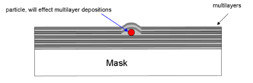
Figure 1.2: A diagram of a non-patterned EUV mask. To fabricate the mask, a blank 6.35 mm thick quartz blank is used to alternatively deposit the reflective layers. If a particle is present, it will perturb the smoothness and effect the mask properties.
EUV Optics Degradation Due to Carbon Contamination
In addition to the mask degradation due to particulate contamination outlined in section 1.3, the high intensity photon irradiation of other components of the system, namely the EUV mirrors which compose the collector array, can become contaminated. It has been shown that the high energy photon interaction with collector mirrors in the presence of background hydrocarbons in the vacuum of the proposed EUV lithography tool will result in a buildup of carbon layers on the mirror [4]. This resulting carbon layer can be cleaned by atomic hydrogen, plasma etching, or through use of molecular oxygen [4]. However, these cleaning techniques can lead to damage of the surface through either physical damage, chemical attack, or oxidation [4].
How PACE Works
When a plasma is formed, energetic ions and electrons are created in the plasma and are typically what are important to the engineer creating the plasma. However, there is a strong energetic neutral component in plasmas too in the form of metastable atoms. Metastable atoms are those that are stuck in a quantum state and are forbidden through conservation of momentum from decaying to the ground state (such as 2s to 1s transitions being forbidden). Thus, any electron entering the 2s state will be hypothetically `stuck.’ In general, the lifetime of these metastable atoms is low, so they don’t often play a significant role. There are two metastable states in helium, singlet 2s and triplet 2s, with 20.616 eV and 19.820 eV of energy each as seen in Figure 3.1 [28, 29] with lifetimes on the order of seconds. Helium plasma has been used for the current work due to its low sputtering threshold on lithographic material (due to its low mass), in order to achieve particle removal. Under some conditions of prior work, namely the electrostatic removal process associated with PACE, a pulsed DC bias was applied to the sample [24]. This same type of processing has been carried forward to the current work due to the pulsed power supply that was previously used able to draw more current. The pulse typically operated between +10 volts and -70 volts at a frequency of 100 Hz at a duty cycle of 90 % positive. This leads to sputtering of the sample at -70 volts for 10 % of the processing time. Section 3.1 outlines the expected removal of three material types from pure sputtering alone which when compared with the preliminary results, does not explain the removal mechanism. Through optical emission spectroscopy, it is possible to monitor the 501.6 nm and 388.9 nm transition that populate the 2s singlet and 2s triplet state respectively. As shown in Figure 3.2 and Figure 3.3, one is able to affect the density of the metastable states in the plasma through both bias to the sample as well as overall plasma source power.
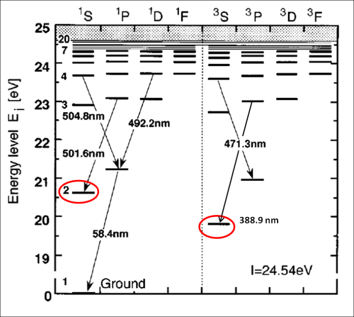
Figure 3.1: A diagram of the energy levels of the helium atom. The two circled levels represent the metastable energy levels which are quantum mechanically forbidden from decaying to the ground state energy due to the conservation of angular momentum. Diagram from Sasaki et. al. [28]
Sputtering of Material
Sputtering yields for incident ions on a variety of surfaces can be determined through simulation via SRIM/TRIM [30]. Figure 3.4 shows the results of this simulation, and specific sputtering yields for 70 eV helium ions are given in Table 3.1 for various materials. The ion current being drawn through the sample is measured to be 1.6 Ǻcm-2. Read More>>